To exploit lucrative market opportunities, satellite operators are trying to differentiate by offering added-value services, e.g. ultra high-resolution imagery, live streaming video and on-board AI to extract insights in-orbit to reduce downlink requirements. The market need for high-throughput payloads is predicted to increase 12x from 2019 to 2024, with bandwidths increasing to 26,500 Gbps.
All of the above applications impact the storage capacity and speed of on-board mass memory. Real-time as well as Store & Forward high-throughput payloads are baselining FPGAs, microprocessors, broadband ADCs and DACs with GHz I/O rates. As an example, a 12-bit ADC sampling at 1.5 GSPS generates 18 Gb of raw data per second. One minute of compressed SAR information requires approximately 70 Gb of storage. These mission needs challenge current space-grade memory solutions in terms of their I/O bandwidth, access time, power consumption, physical size and storage capacity.
A typical architecture of a digital high-throughput payload is shown below and either a space-grade FPGA or a fast microprocessor is used to perform the on-board processing. The latest, ultra deep-submicron, qualified FPGAs typically contain around 30 Mb of on-die memory and CPUs even less. Telecommunication, Earth-Observation and science payloads based on this architecture, planning to use Xilinx’s XQRKU060, Microchip’s RTPolarFire® or NanoXplore’s space-grade FPGAs, will need additional, fast off-chip memory to store the large amounts of data generated by such applications.
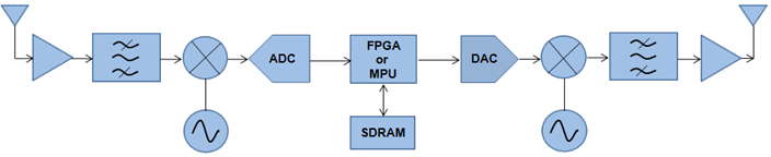
Figure 1 : The architecture of a digital high-throughput payload
Real-time processing, complemented by compression and the storage of large bandwidths of data quickly, is required to deliver the next generation of high-throughput satellite services. The problem is to identify suitable space-grade mass-memory with sufficient capacity, speed and reliability.
The fastest and largest semiconductor technology is SDRAM which is organised as a logical array of cells, with the basic component of storage within each comprising a capacitor and a FET as the control gate. Each cell stores one bit and a simple 4-bit memory is illustrated below. The transistor opens or closes based on the voltage on the row, charging or draining respectively the capacitor attached to it. After the desired ‘word-line’ is charged, the column selector is switched to access the required capacitor for the up-coming read/write operation. Due to its natural discharge, the cells have to refreshed periodically, which involves reading and then re-writing the data back.
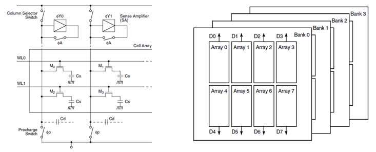
Figure 2 : SDRAM bit cells and the organisation of an SDRAM chip.
SDRAM architecture comprises memory cells organised into a two-dimensional array of rows and columns. To select a particular bit, it is first necessary to address the required row and then the specific column. Once the desired row is open, it is possible to access multiple columns, hence improve speed and reduce latency through successive read/write bursts.
To increase the word size, the memory has multiple arrays which means when a read/write access is requested, the memory only requires one address to access 1 bit from each array.
To increase overall memory capacity, banks are added to the internal structure of SDRAM as illustrated above. Bank interleaving further increases performance and each can be addressed individually.
To perform a read or write, the ACTIVE command first has to be issued by the memory controller to activate the required row and bank. Once the desired operation has completed, the PRECHARGE command closes a particular row in one or more banks. A new row cannot be opened until the previous one has been closed.
SDRAM operation is achieved using its control signals, Chip Select (CS), Data Mask, (DQM), Write Enable (WE), Row Address Strobe (RAS) and Column Address Strobe (CAS), with the last three determining which command is issued as listed below:
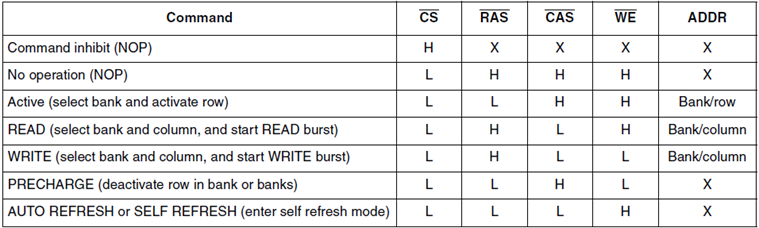
Table 1 : The SDRAM command truth table.
SDRAM has evolved significantly since its release in 1992: the initial version was Single Data Rate (SDR) SDRAM was has the same internal clock frequency and I/O rate. SDR SDRAM can only read or write once in a clock cycle and has to wait for the completion of the current operation before starting the next.
Double Data Rate (DDR) SDRAM achieves greater bandwidth without increasing the clock frequency by transferring data on both clock edges, doubling the I/O transfer speed without increasing the clock frequency. This is accomplished by using a 2n-prefetch architecture where the internal data-path is twice the width of the external bus, allowing the internal frequency to be half the external transfer speed. For each single read access, two external words are fetched and for a write operation, two external data words are combined internally and written in one cycle. DDR1 is a true source-synchronous design, where the data is captured twice per clock period using a bi-directional data strobe.
DDR2 SDRAM operates the external bus twice as fast as DDR1 doubling the I/O transfer rate. This is achieved by using a 4n-prefetch buffer where the internal data-path is four times the width of the external data bus. DDR2 can operate at half the clock frequency of DDR1 and achieve the same transfer speed, or at the same rate with double the information bandwidth.
DDR3 SDRAM operates the external bus twice as fast as DDR2 doubling the I/O transfer rate by using an 8n-prefetch architecture. The width of its internal data-path is eight bits compared to DDR2’s four. DDR3 can operate at half the clock frequency of DDR2 and achieve the same transfer speed, or at the same rate with double the information bandwidth.
Table 1 summarises the space-grade SDRAM options which are currently available to satellite and spacecraft manufacturers.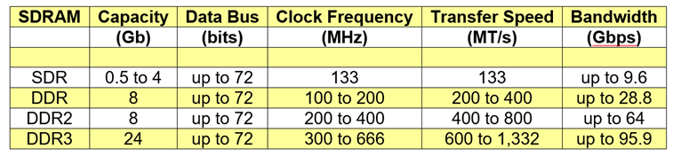
Table 2 : Current, space-grade SDRAM capability.
To deliver the next generation of high-throughput satellite services, future payloads require faster, larger-capacity, physically-smaller and lower-power consuming on-board storage. Small-satellite constellations have specific size and power constraints, and OEMs are seeking higher memory bandwidths to enable real-time applications.
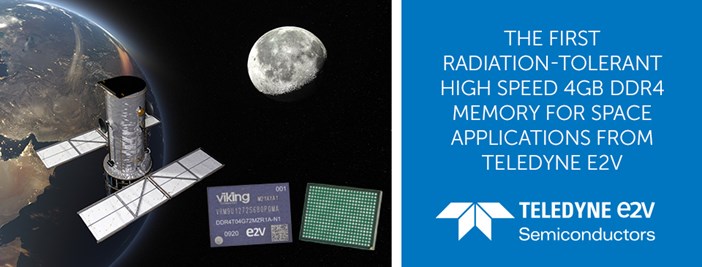
Teledyne-e2v has just released the first, rad-tolerant DDR4 SDRAM for space applications: the DDR4T04G72 is a 72-bit, 4 GB (32 Gb) memory, targeting an I/O speed of 2400 MT/s and an effective bandwidth of 153.6 Gbps with ECC or 172.8 Gbps without. The device is packaged in a compact 15 x 20 x 1.92 mm PBGA containing 391 balls with a pitch of 0.8 mm as shown below. The part can be ordered from -55 to +125 °C or from -40 to + 105 °C, and leaded versions are available up to NASA level 1 and ECSS class 1 qualification. The product roadmap includes a plan to also release an 8 GB (64 Gb) version.
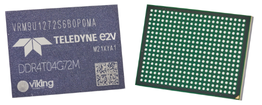
Figure 3 : The rad-tolerant, DDR4T04G72, 4 GB DDR4 memory.
In terms of radiation hardness, the DDR4T04G72 has a specified SEL threshold > 60.8 MeV.cm2/mg, SEU and SEFI thresholds of 8.19 and 2.6 MeV.cm2/mg respectively, and a target TID immunity of 100 krad (Si).
The 4 GB DDR4T04G72 is an MCM containing five die, four of which offer 1GB (8 Gb) of storage each, 512 Mb x 16 bits, organised in two groups with four banks in each. To bolster reliability, a 72-bit data bus is created comprising 64 data and 8 bits for error detection and correction. This ECC function is realised within the fifth die. The device uses an internal 8n-prefetch buffer to maximise high-speed operation and offers programmable read, write and additive latencies.
The typical supply voltage of DDR4 is 1.2 V and the following table compares the typical power consumption and physical size of the DDR4T04G72 with existing space-grade SDRAM. Power dissipation is highly dependent on specific device architecture, the clock frequency, the supply voltage, the operation being performed, the state of the part, e.g. active, pre-charge or read/write, the time spent in each state, whether bank interleaving is used and I/O circuit implementation, e.g. termination. Depending on how your avionics uses SDRAM, power consumption can vary greatly. For system design, it’s important that you consider how the memory is being accessed and driven to specify the PDN and the thermal solution accordingly. DDR4 also includes a 2.5 V rail, VPP, to provide a word-line boost to improve efficiency.
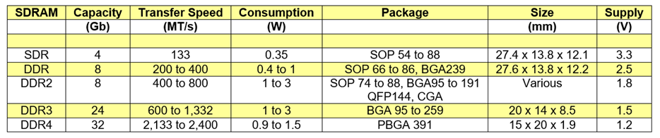
Table 3 : Comparison of space-grade SDRAM capability.
IBIS, SPICE, thermal models and a power-estimator spread-sheet for the DDR4T04G72 are available from Teledyne-e2v. A configuration file can also be provided to generate DDR4 controller IP within the Vivado® Design Suite when the part is paired with Xilinx’s XQRKU060, space-grade FPGA.
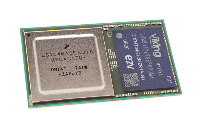
The DDR4T04G72 DDR4 SDRAM can also be procured combined with a rad-tolerant, quad, 64-bit ARM® Cortex® A72 CPU operating at 1.8 GHz on a small, single substrate measuring 44 x 26 mm as shown below. There is currently some discussion as to whether this space-grade module should be offered with leaded or RoHS passives.
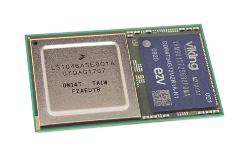
Figure 4 : The rad-tolerant, QLS1046-4GB quad ARM core combined with the DDR4T04G72 DDR4 memory.
DDR4 will allow the satellite industry to offer higher-throughput on-board processing and increased acquisition times enabling new Earth-Observation, space-science and telecommunication applications, e.g. ultra high-resolution imagery, live streaming video and on-board AI.
For the first time, the DDR4T04G72 will allow satellite and spacecraft manufacturers to avail of the large memory bandwidths that have been available to our commercial cousins for the last six years. Compared to existing, qualified DDR3 SDRAM, the DDR4T04G72 can be used with the latest space-grade FPGAs and microprocessors providing:
This article has been written by Dr. Rajan Bedi, the CEO and founder of Spacechips.