When using modern wideband data converters, one substantial challenge is managing the resulting high-speed serial data streams. ESIstream is an open source, serial data interface protocol designed with minimal overhead and delivers a simple hardware implementation within a range of targeted FPGA architectures whilst requiring a minimum of resources. Simply stated, it’s the open source alternative to JEDEC’s JESD204B subclass 1 & 2 standards. But, this simple explanation ignores some significant benefits for ESIstream users. Benefits discussed here include lower complexity, a reduction in link latency and a simpler way to achieve deterministic latency.
This short article concentrates unashamedly on ESIstream’s structure as much existing documentation ably covers the standardized JESD204B. Then we’ll unpack some of the subtle differences between the protocols and introduce news that Teledyne e2v, ESIstream’s protocol developer, have decided to introduce their own ESIstream VHDL IP to further simplify its adoption.
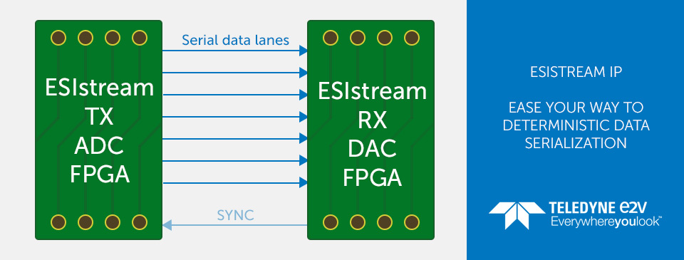
Around the turn of the millennia, advances in data convertor technology as well as CMOS processes was starting to hit functional limits. Originally high-speed ADCs and DACs (fs > 10 MHz) featured parallel data interfaces meaning that a significant number of printed circuit board (PCB) traces had to be run to/from each convertor (figure 1). Furthermore, as sample rates and thus output data rates increased, PCB design became increasingly challenged. Serializing the interface, first with LVDS (low voltage differential signaling) then most recently with Serializer/deserializer (SERDES) interfaces – where the clock is embedded in the data stream promised a solution to this data transmission challenge; they promised simplified PCB layouts and a substantial improvement in form factor. The interface simplification benefits both ends of the link (figure 1). Serdes links helped ease PCB design further as it eliminated the need for the data lane lengths to be matched.
 Figure 1 How serial links reduce the interconnect burden.
However, it has taken many years to have a serial solution which solves all the system level challenges presented by wideband data convertors. Achieving deterministic latency, a prerequisite for simultaneous sampling, has taken a lot of effort to deliver. This is clear from the table below (table 1) that shows the development of both the JESD204 standard over the last 12 or more years as well as the open source ESIstream alternative.
| LVDS | JESD204 | JESD204A | JESD204B SUBCLASS 1 | JESD204B SUBCLASS 2 | ESIstream | |
| Release year | 2001 | 2006 | 2008 | 2011 | 2011 | 2014 |
| Lane rate [Gbps] | 3.125 | 12.5 | 12.5 | 12.8 Gbps (EV12AQ600) Only limited by transceiver. |
||
| Multi-lane synchronization | No | No | Yes | Yes | Yes | Yes |
| Multi-device synchronization | No | Yes | Yes | Yes | Yes | Yes (demonstrated) |
| Deterministic latency | No | No | No | Yes (fs > 500MSPS) |
Yes (fs > 500MSPS) |
Yes |
Among the more obvious benefits of serialized data is that the device package need not include extra data lines even when resolution is increased, helping limit pin count expansion. However, a downside to serialization is extra transmission latency due to the encode/decode process and lane alignment which can be compensated using some extra receive path elastic buffering.
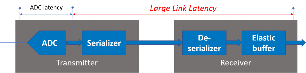 Figure 2 Serialization introduces interconnect latency.
Serializing also helps manage power demand within data convertors as it reduces the number of specialized output drivers a single device requires. Moreover, minimizing electrical noise generated in complex systems to maintain a certain dynamic range is aided by implementing differential serial lines. Coding schemes can also spread spectral noise and furthermore, differential signaling helps minimize crosstalk.
In reality, until recently applications where multiple parallel channels are sampled synchronously have not been well served by early generation serial interfaces leaving developers with some challenging board level design problems.
Now a quick look at the nuts and bolts of ESIstream. ESIstream uses a 14b/16b data encoding algorithm, least significant bit first and supports lane rates in excess of 13 Gbps. It suits 12- and 14-bit resolution converters. The protocol uses a linear feedback shift register scrambling process and adds both a disparity and clock synchronization bits (2 bit overhead) to each data word as shown in figure 3. In this way, its coding efficiency of 87.5% is slightly better than for JESD204B (an 8b/10bit coded stream). The disparity bit (DB) ensures DC balance across the data link whilst the CLK bit is toggled to enable synchronization monitoring.
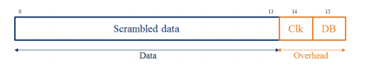 Figure 3 ESIstream basic data frame.
High level block diagrams of the ESIstream transmitter (Tx) and receiver (Rx) cores are shown in figures 4 and 5 below.
 Figure 4 The Tx path of ESIstream.
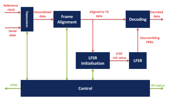 Figure 5 The Rx path of ESIstream.
The ESIstream encoding algorithm has been designed to mitigate the physical limitations of serial interfaces. Most importantly, the link between transmitter and receiver needs to be ac coupled. Given this, it is important that the transmitted data be DC balanced otherwise the link coupling capacitors can drift causing the data eye to close, corrupting received data.
At the receiver, the clock and data recovery (CDR) block usually uses a PLL to lock to the transmitted signal, this eliminates the need for separate clock lines. However, for the CDR to lock and stay locked, a guaranteed number of transitions within the transmitted signal is mandatory.
Scrambling the transmitted data is performed to ensure that both a statistical dc balance is maintained and guarantee that the link will remain locked. The developers of ESIstream wanted to restrict the complexity of the digital design and settled upon an additive algorithm that minimizes error propagation. The resulting algorithm is based on a Fibonacci polynomial with a run length of 217-1. Additionally, a 14- bit shift is applied. The useful data from the conversion process is exclusive ORed with the linear feedback shift register data (a pseudo random code) as depicted in figure 6 below.
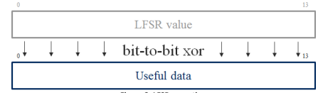 Figure 6 Scrambling data by exclusive ORing with the LSFR code.
After scrambling, the resulting 14 bits of data are encoded into a 16-bit frame. The first overhead bit, the clock bit toggles with every consecutive frame. The second added disparity bit is set depending on the current state of the running disparity counter (RDC). Two RDC situations can result:
1. The RDC is less than +/- 16 and so the disparity bit is set to ‘0’
2. The RDC is more than +/- 16 and so the disparity bit is set to ‘1’ and the data are inverted (bit-to-bit not operation)
This action satisfies the demands of minimal number of transitions for Rx PLL lock and meets the needs for dc balance on the link. Under normal operation, the receiver checks the disparity bit first. If it is set high, then the received data is inverted prior to de-scrambling. With the disparity bit un-asserted the data is directly de-scrambled.
For deterministic operation, ESIstream link set-up demands that the link is synchronized, i.e. data frames are aligned between transmitter and receiver and that the scrambling engines on both side of the link are in the same initial state. Synchronization works in two steps; frame alignment and pseudo-random bit sequence (PRBS) initialization.
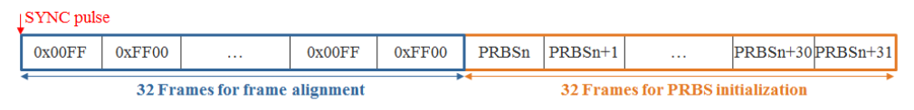 Figure 7 ESIstream Link synchronization frames.
The receiver initiates the process by asserting SYNC. The pulse should last at least one frame period. The transmitter then sends a 32-frame alignment pattern (figure 5). This reserved sequence bypasses scrambling and disparity processing at the receiver, time aligning the receiver to the transmitter. Immediately after the alignment frames, the transmitter sends a further 32 frames of PRBS data – comprising 14-bits of PRBS plus clock and disparity information. Correctly processed, the receiver LFSR is initiated with the receiver PRBS words. At this point the link/s is/are synchronized (figure 8). Synchronization can be continuously monitored in the receiver by observing the clock bit. If it fails to toggle on each frame, then there is a synchronization problem and the link should be reset and re-synchronized.
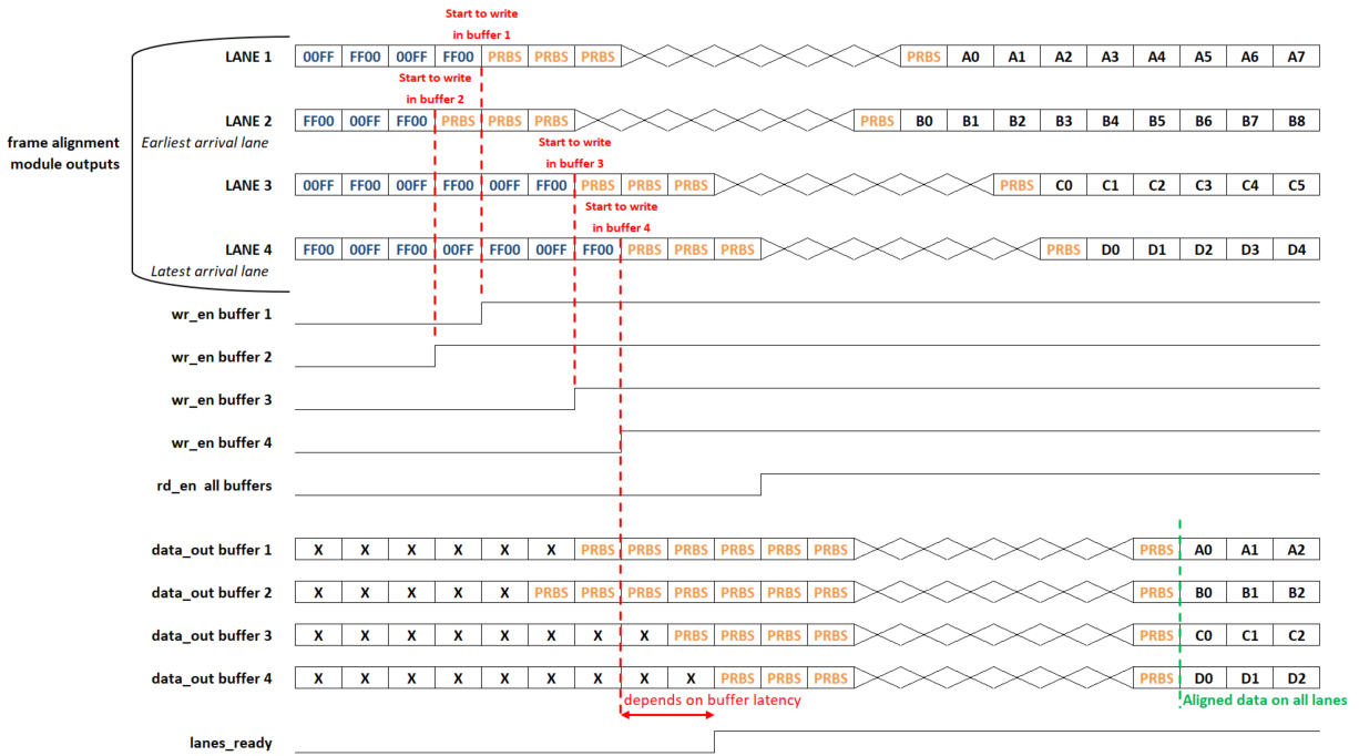 Figure 8 ESIstream receiver lanes synchronization sequence.
With scrambling, clock and disparity bit processing, deterministic data transmission over ESIstream is ensured.
The principle of interference as applied in digital beamforming to radio systems requires antenna arrays whose low-level signals are sampled simultaneously. This preserves spatial information as signals arrive at each antenna node. Though there’s a complexity and power penalty to this approach, several worthwhile benefits arise:
Today, many applications use beamforming, or at least demand synchronous sampling. However, operating at gigahertz frequencies, signal propagation times become important both at the IC and board level. PCB traces act as transmission lines and it is thus critical that signal trace lengths are matched to retain phase information. A centimetre of trace adds between 60 to 75ps of travel time. Compare that to the clock period of 166ps for a 6 GHz sample clock. Therefore, board level effects significantly influence the design. This explains why PCB layout is a critical success factor in high speed sampling systems. However, there is one other factor that makes life difficult and that’s one tied to the digital domain; referred to as metastability.
Metastability describes an uncertain state in digital electronics and as sample rates increase it becomes one of the prime sources of potential system timing problems. A synchronization method is required as a counter to metastability and that’s where SYNC chaining comes in.
A robust and easy to implement method to synchronize timing is thus to be welcomed. At Teledyne e2v, deterministic synchronization is built around a pair of event driven, differential electrical signals; the SYNC and sync-output signals (SYNCTRIG and SYNCO). Between them, these signals ensure that the timing system of a target converter can be reset, and that all digital sub-systems are properly locked to the reference master clock. Moreover, this synchronization can then be extended to ADCs throughout the larger system.
The benefits of this approach are its relative simplicity – it requires no extra clock signal yet guarantees synchronization across many parallel channels over the lifetime of the system. Once a design is finalized and is production ready, a single training cycle establishes correct system synchronization. If environmental conditions change, such as temperature or voltage, system timing parameters remain fixed. The SYNC chain provides a rock solid, synchronization source – a major benefit when moving into mass production.
Then, to achieve deterministic latency, on the receive end of the ESIstream link, there is a simple counter associated with the receive elastic buffer which can compensate for the maximum individual lane latency uncertainty of the transmission.
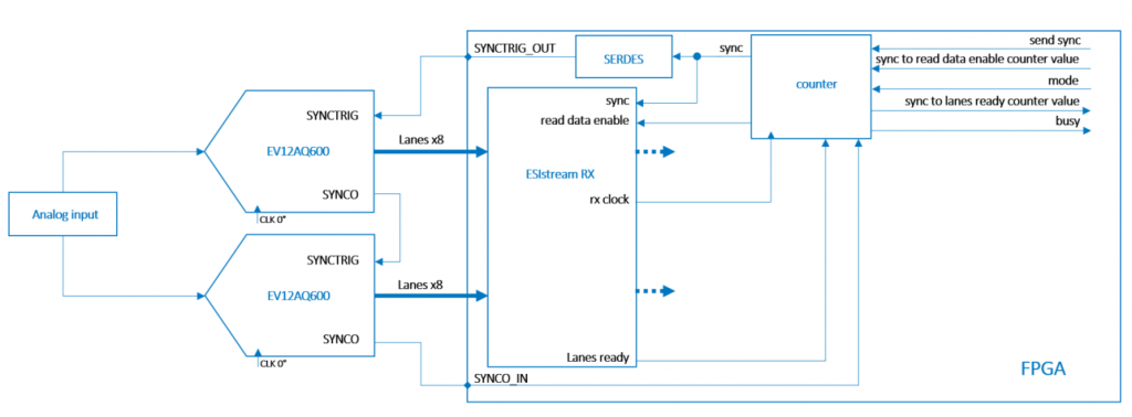 Figure 9 Showing the frame counter position in the ESIstream receiver.
The counter module embedded in the FPGA counts the number of Rx clocks between the SYNCTRIG rising edge event and the ‘all lanes received ready’ event. This information combined with elastic receive buffering allows for the deterministic alignment of received data across the whole system. Thus, expanding that deterministic behavior throughout an ESIstream equipped system is a relatively modest task due to a feature built into ESIstream equipped products namely the SYNC chain.
Making ESIstream truly easy to adopt, Teledyne e2v the originators of ESIstream, initiated a project in late 2018 to source ESIstream Tx and Rx IP blocks for use with industry standard FPGAs from companies including Xilinx and Intel. The IP will be suitable for operation at different speed and qualification levels including for space applications. Unsurprisingly, IP is focused initially on providing matched performance with existing devices within Teledyne e2v’s product portfolio. However, in addition to this fixed function IP, work is underway to define dynamically reconfigurable line rate modules covering a broad range of data converter sample rate frequencies providing even more customer utility.
Future oriented development activities at Teledyne e2v also include the application of fibre-optics for the ESIstream physical layer. Fibre-optics allows converters to be located a greater distance from the FPGA than using copper-based interfaces (PCB traces or coaxial cables). This capability is already demonstrated in the connection of two Xilinx VC709 evaluation boards connected via four SFP (small form factor pluggable) optical lanes each running at 6 Gsps.
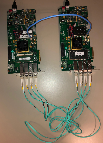 Figure 9 ESIstream Tx and Rx demonstration using fibre-optics for the physical layer.
VHDL code modules will be made available once they have been fully qualified by the company from their website as a freely downloadable resource.
Recapping the system level benefits of ESIstream, are:
| JESD204B | ESIstream |
| Industry standard | Open source |
| Off the shelf IP | VHDL Code modules |
| Flexible (adds overhead and power) | Lower resource & protocol overheads. |
| Deterministic latency (with added hardware complexity e.g. SYSREF) | Deterministic latency |
| Direct sample & data clock relationship (CLK overhead bit) | |
| Lower link latency | |
| No IP license fees | |
| Reduced power |
The JEDEC data serialization approach described in JESD204B sub-classes 1 & 2 appears to have solved the challenge of achieving deterministic operation of multi-channel data convertor systems. Whilst this is no doubt partially true, what is often missed in an initial inspection of the standard are the very many challenges designers face to handle the complex transport and physical layer requirements of the specification.
Engineers may rightfully expect that acquiring a JESD204B license and the core IP for the link embedded in their signal processing SoC (FPGA or ASIC) removes most of the system design challenges. However, reported real world experiences demonstrate that the timing constraints imposed by the multi-domain clock complexity of JESD204B ties considerable development resources up in getting the PCB design just right.
There is another way. ESIstream. ESIstream is open source, free for all to use. It matches the performance levels provided by JESD204B but offers a superior user experience. Less complexity, easier design, reduced power. Now, with the introduction and availability of trusted IP blocks and VHDL code modules for both Rx and Tx blocks compatible with industry standard FPGAs, ESIstream eliminates the last barrier to use. IP blocks are under development to match the specification of new data convertors from Teledyne e2v. Furthermore, customers are free to download VHDL code modules for their own high-speed serial projects.
Notes to Editors:
About Teledyne e2v
Teledyne e2v’s innovations lead developments in healthcare, life sciences, space, transportation, defence and security and industrial markets. Teledyne e2v’s unique approach involves listening to the market and application challenges of customers and collaborating with them to provide innovative standard, semi-custom or fully custom solutions, bringing increased value to their systems. Teledyne e2v is a world leader in re-engineering and up-screening commercial technologies and has held a strategic partnership with NXP for over 30 years to develop space, military and industrial grade versions of NXP’s commercial processors. With access to original test vectors, Teledyne e2v offers guaranteed extended reliability versions of a broad line of the QorIQ® Power® Architecture based portfolio and is developing solutions based on NXP’s Layerscape Series.
For more information, please visit: https://www.esistream.com