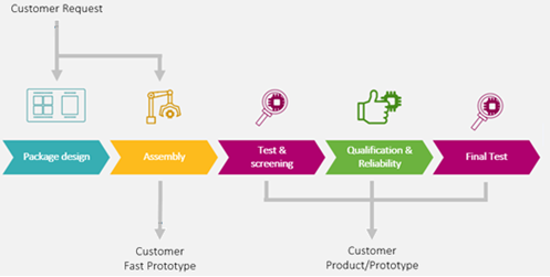
Through the breadth of capabilities that Teledyne e2v Semiconductors can draw upon, our team can attend to all aspects associated with the development and manufacturing of microelectronics solutions. The result is a trouble-free turnkey solution. As well as assembly, there is also scope for customized packaging designs to be implemented where necessary (so that limited available board space can be utilized more efficiently). After these stages have been completed, thermal and electrical simulation activities can be executed. Those are followed for comprehensive testing and finally qualification.
By dealing with everything via just a single source, rather than having to work with multiple partners, Teledyne e2v Semiconductors customers can avoid all the difficulties that will arise from having to manage suppliers for each different step of the process and the coordination of their respective activities.
The vast scope of Teledyne e2v Semiconductors’ capabilities come from the continued investment made in the latest equipment and state-of-the-art facilities. We have a Class 100 cleanroom fitted with advanced tools for wire bonding and flip-chip assembly, as well as multi-zone baking ovens and an extensive array of items of test instrumentation. Equipment is constantly being updated, in order to maintain maximum effectiveness , and a major refurbishment of the cleanroom is currently underway.
Teledyne e2v Semiconductors has attained AS9100 aerospace quality certification, and fully conforms to the standards outlined by both NASA and ESA. As well as ESCC 9000 compliance, we are aligned with QML Class V radiation tolerance for space applications. In addition, we meet the requirements of QML Class Q for qualification of hermetical components in avionics/military applications, plus QML Class Y (MIL-PRF-38535) for non-hermetical flip-chip components employed in such use cases - making us the only facility in Europe (and just one of three in the whole world) with this qualification. In addition, we adhere to the ISO 13485 medical certification requirements.
Our wafer banking capabilities are another important differentiator. These ensure the continued supply of constituent semiconductor devices, so that the risk of obsolescence can be avoided - which is vital for systems designs that can end up being deployed for several decades (such as those used in military applications). Not only does this encompass the ongoing storage of wafers, it also covers the retaining and upkeep of the relevant testers too.
Please fill out & submit the form to receive an answer from our Sales Team or Application Engineers.